TSMC Interview Preparation and Recruitment Process


About TSMC


TSMC (Taiwan Semiconductor Manufacturing Company) is the world's largest dedicated independent semiconductor foundry. Here's a breakdown of what that means and other key aspects:

TSMC Interview Questions

Basic Information

  • Full Name: Taiwan Semiconductor Manufacturing Company Limited

  • Founded: 1987

  • Founder: Morris Chang

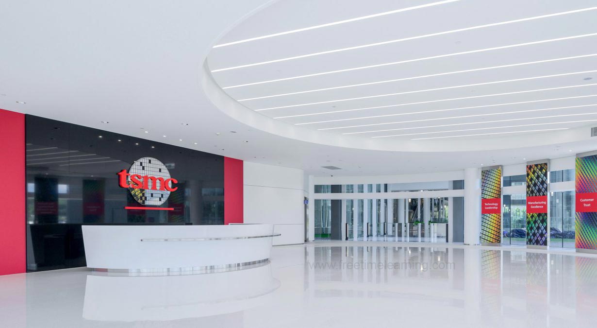
  • Headquarters: Hsinchu Science Park, Hsinchu, Taiwan

  • CEO (as of 2024): C. C. Wei

  • Ticker Symbol: TSM (listed on the NYSE and TWSE)


Core Business


TSMC is a pure-play foundry, meaning it manufactures semiconductors exclusively for other companies and does not design its own chips. This business model has enabled it to work with many major clients.


Major Clients

  • Apple

  • AMD

  • NVIDIA

  • Qualcomm

  • MediaTek

  • Broadcom

  • Intel (increasingly relying on TSMC for advanced nodes)


Technology Leadership

  • TSMC is the first to mass-produce chips at advanced nodes such as:

    • 7nm (2018)

    • 5nm (2020)

    • 3nm (2022–2023)

    • 2nm is under development (expected around 2025)

  • Specializes in FinFET and now moving into GAA (Gate-All-Around) transistor technology.


Global Manufacturing Footprint

  • Main fabs in Taiwan

  • New fabs in:

    • Arizona, USA (TSMC Arizona, focused on 5nm/4nm and 3nm in future)

    • Japan (joint venture with Sony for mature nodes like 22/28nm)

    • Germany (planned)


Why TSMC Matters

  • TSMC is critical to the global tech supply chain, producing chips for everything from iPhones to AI servers.

  • It accounts for over 50% of the global foundry market.

  • It plays a major role in geopolitics due to its location in Taiwan and the strategic importance of its technology.


Recent Developments (as of 2024-2025)

  • Increasing investment in AI chips due to demand from NVIDIA and others.

  • Facing challenges in global expansion due to workforce training and local infrastructure.

  • Working on 2nm node with nanosheet (GAA) transistors.


TSMC Recruitment Process


The TSMC recruitment process is structured to evaluate both technical depth and cultural fit, especially for roles in engineering, R&D, and manufacturing. Here's a breakdown of the typical process:

TSMC Recruitment Process (for Engineering & Technical Roles)


1. Application

  • Submit via:

    • TSMC career portal

    • LinkedIn or job fairs (especially in Taiwan and universities globally)

    • Campus recruitment for fresh graduates (very active in Taiwan, US, and top Asian universities)


2. Resume Screening

  • Reviewed by HR and the technical hiring team

  • Strong emphasis on:

    • Semiconductor or electronics background

    • Academic performance (GPA matters, especially in Taiwan)

    • Internships, research, or experience with VLSI, CMOS, fab, etc.


3. Online Test / Technical Assessment

This may include:

  • Aptitude tests (math, logic, reasoning)

  • Technical MCQs related to:

    • Digital & Analog electronics

    • Semiconductor Physics

    • CMOS, VLSI Design

    • Process Integration, Device Physics

  • Coding test (for software-related roles only)


4. Technical Interviews (1–3 Rounds)

Topics vary by role:

  • Process Engineer / R&D Engineer:

    • Semiconductor fabrication (etching, lithography, deposition)

    • Device Physics (MOSFET characteristics, scaling)

    • Process integration knowledge

  • Design Engineer / DFT / Verification:

    • Digital design, RTL coding (Verilog/VHDL)

    • Timing, STA, testability

    • Scripting (Python, Perl, TCL)

  • Software/EDA Engineer:

    • Data structures, algorithms

    • System design, scripting

    • EDA tools (e.g., Synopsys, Cadence)

Interviewers focus on problem-solving skills and depth of understanding, not just surface-level knowledge.


5. HR Interview

  • Behavioral and fit assessment

  • Questions may include:

    • Why TSMC?

    • How do you handle stress in a high-pressure environment?

    • Are you open to working in shift-based roles or relocating?


6. Offer and Onboarding

  • Offers include:

    • Competitive salary (especially in Taiwan and US)

    • Relocation support

    • Benefits like health insurance, housing allowance (in Taiwan)

TSMC Interview Questions :

1 .
Explain the key steps in semiconductor manufacturing.
Semiconductor manufacturing begins with wafer preparation, where high-purity silicon crystals are grown, sliced, and polished. Next, oxidation forms a silicon dioxide layer for insulation. 

* Photolithography transfers circuit patterns onto the wafer using UV light and photoresist. 

* Etching (wet/dry) removes unwanted material to create features. 

* Doping (ion implantation/diffusion) introduces impurities to adjust conductivity. 

* Thin-film deposition (CVD, PVD, ALD) adds dielectric or metal layers. 

* Chemical mechanical planarization (CMP) smoothens surfaces. 

* Metallization forms interconnects via copper damascene.

Finally, testing (electrical probes) and packaging (dicing, bonding) complete the process. Each layer repeats these steps to build complex ICs.
2 .
What is photolithography, and what challenges arise at advanced nodes?
Photolithography uses light to transfer patterns from a mask to a photoresist-coated wafer. At advanced nodes (e.g., 5nm), challenges include diffraction limits due to shorter wavelengths, requiring immersion lithography or EUV (13.5nm).

* Multi-patterning (double/quadruple patterning) increases complexity and cost.

* Overlay accuracy becomes critical as feature alignment tolerances shrink to nanometers. Photoresist sensitivity and line-edge roughness also impact resolution.

Defects from particulate contamination or mask errors escalate yield loss. Solutions involve advanced masks (phase-shift), computational lithography, and tighter process controls to maintain pattern fidelity and throughput.
3 .
What are the advantages of EUV lithography?
EUV lithography uses 13.5nm wavelength light, enabling smaller feature sizes without multi-patterning, reducing process steps and costs. It improves pattern resolution and fidelity for sub-7nm nodes. EUV’s shorter wavelength minimizes diffraction, allowing precise critical dimensions (CDs).

However, challenges include low 
source power (tin plasma), mask defects due to reflective multilayers, and resist sensitivity. TSMC adopted EUV for 7nm+ nodes to simplify metal and via patterning, enhancing density and performance. Despite high tool costs, EUV is critical for scaling beyond 3nm.
4 .
Compare FinFET and planar transistors.
FinFETs use a 3D fin structure, increasing gate-channel contact area for better electrostatic control, reducing leakage and short-channel effects. This allows lower voltage operation and higher density. 

Planar transistors suffer from gate oxide leakage at sub-20nm nodes due to reduced gate control. FinFETs also enable higher drive current and scalability to 5nm.

However, FinFET fabrication is complex, requiring precise fin etching and doping. TSMC transitioned to FinFET at 16nm, while planar was used up to 28nm. Future nodes (3nm) may use 
GAAFETs (gate-all-around) for further scaling.
5 .
How does doping affect semiconductor properties?
Doping introduces impurities (e.g., phosphorus for n-type, boron for p-type) to modify silicon’s conductivity. Ion implantation accelerates dopant ions into the lattice, followed by annealing to activate them. Doping creates p-n junctions for transistors and adjusts threshold voltages.

High doping concentrations increase carrier mobility but risk defects like dislocation. Challenges include 
channeling effects during implantation and diffusion during thermal steps. Advanced nodes use halo doping to mitigate short-channel effects. Dopant placement precision is critical for performance and leakage control.
6 .
What is CMP, and why is it critical?
Chemical mechanical planarization (CMP) combines chemical etching and mechanical polishing to flatten wafer surfaces. Slurries (abrasives + chemicals) remove excess material (e.g., copper, oxide) post-deposition. CMP ensures uniform layers for photolithography and prevents topography-induced defects.

It’s vital for 
multi-layer interconnects, enabling precise depth-of-focus in lithography. Challenges include dishing, erosion, and slurry residue. TSMC optimizes CMP with in-situ metrology to maintain planarity, critical for advanced nodes where even nanometer-level variations affect yield.
7 .
Discuss thermal budget in fabrication and minimization strategies.
Thermal budget refers to cumulative heat exposure during processing. High temperatures cause dopant diffusion, degrading junction abruptness. Minimization strategies: Rapid thermal processing (RTP) for short anneals, laser annealing for localized heating, and low-temperature deposition (e.g., ALD).

Advanced nodes use 
spike annealing to activate dopants without excessive diffusion. Lower thermal budgets preserve shallow junctions and prevent material degradation (e.g., high-k dielectrics). TSMC employs these techniques to maintain device performance at 5nm and below.
8 .
What are common wafer defects, and how are they detected?
Defects include particles (contamination), crystallographic defects (dislocations), and pattern errors (bridging, misalignment). Detection methods: Optical inspection (brightfield/darkfield), SEM for sub-micron defects, and TEM for atomic-level analysis. 

E-beam inspection offers high resolution but slower throughput. In-line metrology (scatterometry, AFM) monitors critical dimensions. TSMC uses automated defect classification (ADC) and machine learning to prioritize yield-critical defects. Early detection reduces scrap and improves process control.
9 .
Explain the significance of gate oxide in MOSFETs.
The gate oxide (traditionally SiO₂) insulates the gate from the channel. Thinner oxides improve gate control but increase tunneling leakage. At sub-28nm nodes, high-k dielectrics (e.g., HfO₂) replace SiO₂, offering higher dielectric constants (k=20-25 vs. 3.9) for equivalent capacitance with thicker layers, reducing leakage. Metal gates (e.g., TiN) eliminate poly-Si depletion, enhancing drive current. TSMC introduced high-k/metal gates at 28nm, critical for power efficiency and scaling.
10 .
What is Design for Manufacturability (DFM)?
DFM involves designing ICs to simplify fabrication and improve yield. Techniques include OPC (optical proximity correction) for lithography, dummy fill to ensure uniform CMP, and redundant vias for reliability. TSMC collaborates with designers on design rules (min spacing, width) and provides process-specific PDKs (process design kits). DFM reduces variability from lithography, etching, and CMP, ensuring functionality across process corners. It’s vital for advanced nodes where marginalities are tighter.
11 .
How to reduce process variation in manufacturing?
Statistical process control (SPC) monitors tool parameters (e.g., etch rate, temperature) to detect drifts. Advanced process control (APC) uses real-time feedback/feedforward adjustments. Equipment matching ensures uniformity across tools. 

Design rules account for lithography limitations (e.g., forbidden pitches). TSMC employs machine learning to predict and correct variation sources, such as overlay errors or CMP non-uniformity. Reducing variation improves yield and device performance consistency.
12 .
What is shallow trench isolation (STI)?
STI isolates transistors by etching trenches between active areas and filling them with oxide (SiO₂). It replaces LOCOS (local oxidation) for better planarity and scalability. STI prevents latch-up by reducing parasitic bipolar transistor formation. Challenges include stress-induced defects and trench aspect ratios. TSMC optimizes STI with high-density plasma etching and CMP to ensure isolation at sub-7nm nodes.
13 .
Discuss electromigration and mitigation techniques.
Electromigration is metal atom migration due to high current density, causing voids (opens) or hillocks (shorts). Mitigation: Copper interconnects (higher EM resistance than Al), barrier layers (Ta/TaN), and redundant vias. Design rules limit current density and use wider lines for critical nets. TSMC’s Cu damascene process and advanced alloys (e.g., CoWP capping) enhance EM reliability in advanced nodes.
14 .
Role of metrology in semiconductor manufacturing.
Metrology measures critical dimensions (CD), overlay, film thickness, and defects. Tools include CD-SEMscatterometry, and X-ray reflectometry (XRR). In-line metrology enables real-time process adjustments, ensuring compliance with specs. TSMC uses hybrid metrology (combining multiple techniques) for accuracy, essential for EUV and multi-patterning layers.
15 .
What parameters affect plasma etching?
Plasma etching depends on gas chemistry (e.g., Cl₂ for Si, CF₄ for oxide), RF power (ion energy), pressure (mean free path), and temperature.

Selectivity (target vs. mask material) and anisotropy (vertical profiles) are optimized by balancing chemical (radicals) and physical (ion bombardment) etching. TSMC tunes parameters for each material (e.g., high-k dielectrics require specialized gases) to achieve precise CD control.
16 .
Role of high-k metal gates in CMOS.
High-k dielectrics (e.g., HfO₂) reduce gate leakage by replacing SiO₂. Metal gates (e.g., TiN) eliminate poly-Si depletion, improving drive current. Integration challenges include threshold voltage tuning and interfacial layer control. TSMC’s gate-last (HKMG-last) approach at 28nm enhanced performance and power efficiency, critical for mobile processors.
17 .
Advantages of reactive ion etching (RIE).
RIE combines chemical reactions and ion bombardment for anisotropic etching, enabling high-aspect-ratio features. It offers better CD control than wet etching. Parameters like gas flow and bias voltage adjust selectivity and profile. TSMC uses RIE for gate, contact, and via etching, essential for FinFET and 3D NAND structures.
18 .
How does strain engineering improve transistor performance?
Strain engineering introduces compressive/tensile stress to enhance carrier mobility. Techniques: SiGe source/drain (pMOS) induces compressive stress, stress liners (SiN) for tensile (nMOS). TSMC’s strained silicon at 90nm boosted drive current by 10-30%, critical for speed and power efficiency.
19 .
Benefits of atomic layer deposition (ALD).
ALD provides atomic-level thickness control and conformal coatings, ideal for high-aspect-ratio structures (e.g., FinFET gates). It’s used for high-k dielectrics, metal gates, and barriers. TSMC leverages ALD for precise film uniformity, reducing defects in advanced nodes.
20 .
Challenges in 3D IC packaging.
Challenges include thermal management (heat dissipation in stacked dies), through-silicon vias (TSVs) stress, alignment precision for bonding, and testing complexity. TSMC’s CoWoS (Chip-on-Wafer-on-Substrate) addresses these with advanced materials and design tools, enabling HBM integration in AI chips.
21 .
Importance of cleanrooms in semiconductor fabs.
Cleanrooms control particulate contamination (ISO Class 1-3), using HEPA filters, laminar airflow, and strict gowning protocols. Particles >1/10th the feature size can cause defects. TSMC’s fabs maintain ultra-low contamination levels, critical for yield at nodes below 10nm.
22 .
Failure analysis techniques for semiconductor devices.
Techniques include SEM/TEM for imaging defects, FIB for cross-sectioning, EDX for elemental analysis, and emission microscopy for locating leakage paths. TSMC’s FA labs use nanoprobing and thermal laser stimulation to isolate failures, enabling rapid root-cause analysis.
23 .
Role of interconnects in ICs.
Interconnects (Cu damascene) link transistors, with low-k dielectrics reducing capacitance. RC delay dominates performance at advanced nodes. TSMC uses air gaps and ultra-low-k materials (k=2.4) to minimize parasitics, enhancing speed and power efficiency.
24 .
How to improve yield in semiconductor manufacturing?
Yield improvement involves defect reduction (CMP optimization), process window enhancement (lithography tuning), and design redundancy (ECC, spare cells). TSMC employs AI-driven defect classification and SPC to achieve >90% yields at 5nm.
25 .
Impact of parasitic capacitance in advanced nodes.
Parasitic capacitance between interconnects and gates increases RC delay and power consumption. Mitigation: Low-k dielectricsair gaps, and optimal layout (wider spacing). TSMC’s 3nm node uses hybrid bonding and novel dielectrics to reduce capacitance by 20%, improving performance.
26 .
Give an example of a time when you worked under pressure, how did you handle it?
In my last position as an engineer at a software company, I was tasked with creating a new program that would allow users to create their own website. The deadline for completion of the project was two weeks away, but I knew that if I worked on it full-time, I wouldn’t have enough time to complete it. So, instead, I decided to work on it part-time while also working on other projects. After one week, I had completed 50% of the project. Then, after another week, I finished the rest of the project.
27 .
Tell me about a time when you had to work as part of a team to accomplish a goal.
At my previous job, I was part of a small team that had to complete a project in two weeks. We all met every morning at 8 a.m. to discuss our progress and any challenges we were facing. Each day, we would check in with each other on our progress before leaving for the day. This helped us stay organized and motivated to meet our deadline.
28 .
Why are you looking to leave your current company?
I’m looking for new opportunities because I feel like my current position is no longer challenging enough for me. I’ve been working as an engineer for five years now, and while I love what I do, I think I could use a change of pace. I’m excited about the prospect of learning new processes and techniques with TSMC.