Google News
logo
ECE : Analog Electronics - Quiz(MCQ)
A)
Peak Inverse Voltage
B)
Peak Inferior Voltage
C)
Peak Internal Voltage
D)
Problematic Inverse Voltage

Correct Answer :   Peak Inverse Voltage


Explanation : PIV stands for Peak Inverse Voltage. It is the maximum reverse bias voltage which a diode can bear without breakdown.

A)
Maximum power allowable to a diode
B)
Minimum potential required by a diode to reach conduction state
C)
Maximum reverse bias potential which can be applied across a diode without breakdown
D)
Maximum forward bias potential which can be applied across a diode without breakdown

Correct Answer :   Maximum reverse bias potential which can be applied across a diode without breakdown


Explanation : PIV rating indicates the maximum allowable reverse bias voltage which can be safely applied to a diode. If a reverse potential is greater than PIV rating then the diode will enter reverse breakdown region.

A)
Wien bridge
B)
Hartley
C)
RC phase shift
D)
Both (A) and (C)

Correct Answer :   Hartley


Explanation : Only LC oscillators are suitable for MHz range.

A)
resistor between source and load
B)
inductor between source and load
C)
Both (A) and (B)
D)
capacitor between source and load

Correct Answer :   capacitor between source and load

A)
Current controlled Current source
B)
Current controlled voltage source
C)
Voltage controlled current source
D)
Voltage controlled voltage source

Correct Answer :   Voltage controlled current source

A)
25%
B)
50%
C)
75%
D)
99%

Correct Answer :   25%

7 .
In a p+n junction diode under reverse bias, the magnitude of electric field is maximum at
A)
The edge of the depletion region on the p-side
B)
The p+n junction
C)
The edge of the depletion region on the n-side
D)
The center of the depletion region on the n-side

Correct Answer :   The p+n junction

A)
Unbiased state
B)
Reverse biased state
C)
Forward biased state
D)
It is applicable in all bias states

Correct Answer :   It is applicable in all bias states


Explanation : Diode equation is I=IO(eqV/kT – 1). It is applicable in all bias condition that is forward, reverse and unbiased states.

A)
0.26mV
B)
26mV
C)
36mV
D)
260mV

Correct Answer :   26mV


Explanation : Voltage equivalent of temperature VT is equal to the product of Boltzman constant (J.K-1) and temperature in Kelvin. At a temperature of 27°C, it’s value is VT=KT/q=26mV.

A)
Cut-in voltage decreases
B)
Cut-in voltage increases
C)
Cut-in voltage either increases or decreases
D)
Cut-in voltage doesn’t depend on temperature

Correct Answer :   Cut-in voltage decreases


Explanation : As temperature increases the conductivity of a semiconductor increases. The diode conducts smaller voltage at larger temperature. Therefore, cut-in voltage decreases.

A)
Increases
B)
Decreases
C)
Doesn’t depend on temperature
D)
Either increases or decreases

Correct Answer :   Increases


Explanation : As temperature increases the conductivity of a semiconductor increases. Reverse saturation current increases as temperature increases.

12 .
For a base current of 10 μA, what is the value of collector current in common emitter if βdc = 100
A)
100 μA
B)
10 μA
C)
10 mA
D)
1 mA

Correct Answer :   1 mA


Explaination :

IC = 10 x 100 μA = 1 mA.

13 .
An RC coupled amplifier has an open loop gain of 200 and a lower cutoff frequency of 50 Hz. If negative feedback with β = 0.1 is used, the lower cut off frequency will be
A)
about 2.38 Hz
B)
about 5 Hz
C)
about 50 Hz
D)
about 70.5 Hz

Correct Answer :   about 2.38 Hz


Explaination : New lower cutoff frequency 50 / 1+200x0.1

14 .
The load impedance ZL of a CE amplifier has R and L in series. The phase difference between output and input will be
A)
B)
180°
C)
more than 90° but less than 180°
D)
more than 180° but less than 270°

Correct Answer :   more than 180° but less than 270°


Explaination : It is 180° for purely resistive load and between 180° and 270° for R-L load.

15 .
A constant current signal across a parallel RLC circuits gives an output of 1.4v at the signal frequency of 3.89KHZ and 4.1KHZ. At the frequency of 4KHZ, the output voltage will be
A)
1 v
B)
2 v
C)
1.4 v
D)
2.8 v

Correct Answer :   2 v

A)
Depletion capacitance
B)
Junction capacitance
C)
Channel length modulation
D)
Charge storage capacitance

Correct Answer :   Channel length modulation

A)
CB-CC
B)
CE-CB
C)
CC-CB
D)
CE-CC

Correct Answer :   CE-CB

18 .
An npn BJT has gm = 38 mA/v, Cµ = 10-14 F, Cπ = 4 × 10-13 F and DC current gain β0 = 90. For this transistor fT & fβ are
A)
B)
C)
D)

Correct Answer :   fT = 1.47 x 10¹⁰ Hz & fβ = 1.64 x 10⁸ Hz

A)
Increases noise
B)
Reduces bandwidth
C)
Increase frequency &phase distortion
D)
Reduces gain

Correct Answer :   Reduces gain

20 .
Calculate the reverse saturation current of a diode if the current at 0.2V forward bias is 0.1mA at a temperature of 25°C and the ideality factor is 1.5.
A)
5.5x 10⁻¹⁰ A
B)
5.5x 10⁻⁹ A
C)
5.5x 10⁻⁷ A
D)
5.5x 10⁻⁸ A

Correct Answer :   5.5x 10⁻⁷ A


Explaination : I=I0×(e(V/ηVT) – 1) where I0 = reverse saturation current
η = ideality factor
VT = thermal voltage
V = applied voltage
Here, I = 0.1mA, η = 1.5, V = 0.2V, VT = TK/11600
Therefore, VT at T = 25+273=298 is 298/11600 = 0.0256V.
Therefore, reverse saturation currentReverse saturation current calculation
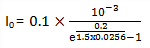
IO=0.00055mA = 5.5×10⁻⁷A.

21 .
Find the applied voltage on a forward biased diode if the current is 1mA and reverse saturation current is 10-10. Temperature is 25°C and takes ideality factor as 1.5.
A)
0.526V
B)
0.618V
C)
0.658V
D)
0.726V

Correct Answer :   0.618V


Explaination : I=I0×(e(V/ηVT)-1) where I0 = reverse saturation current
η = ideality factor
VT = thermal voltage
V = applied voltage
VT at T = 25+273=298 is 298/11600 = 0.0256V, η = 1.5, I = 1mA, I0 = 10-10A
Applied voltage equation with calculation

22 .
If current of a diode changes from 1mA to 10mA what will be the change in voltage across the diode. The ideality factor of diode is 1.2.
A)
7.18V
B)
0.718V
C)
0.0718V
D)
0.00728V

Correct Answer :   0.0718V


Explaination : η = 1.2, I2 = 10mA, I1 = 1mA and take VT = 0.026V

A)
The point of V-I graph where slope is 0.5
B)
The point at which current equal to voltage
C)
Operating point of device
D)
The point at which device have maximum functionality

Correct Answer :   Operating point of device


Explanation : Quiescent point of a device represents operating point of a device. For a diode quiescent point is determined by constant DC current through the diode. The Q-point is the DC voltage or current at a specified terminal of an active device with no input applied. A bias circuit is used to supply this steady voltage/current.

A)
AC resistance
B)
Nominal resistance
C)
Minimum impedance
D)
Maximum dynamic resistance

Correct Answer :   AC resistance


Explanation : Reciprocal of slope of I-V graph at q-point gives AC or dynamic resistance. The inverse of slope will be change in voltage by change in current which is known as dynamic resistance.

A)
Increase
B)
Decrease
C)
Either increase or decrease
D)
None of the above

Correct Answer :   Decrease


Explanation : Slope of I-V graph at q-point is reciprocal of dynamic or AC resistance. Therefore, as slope increases resistance decreases.

A)
Always Equal
B)
Never equal
C)
Both represents same quantity
D)
Calculated from V-I graph

Correct Answer :   Calculated from V-I graph


Explanation : Average AC resistance and dynamic or AC resistance are not exactly the same. They both measure the resistance in different ways. AC resistance is slope of the tangent of the curve of characteristic graph at Q-point. But average AC resistance is measured by measuring the slope of straight line between the limits of operation.

A)
Slightly decreases
B)
Slightly increases
C)
Decreases exponentially
D)
Increases exponentially

Correct Answer :   Decreases exponentially


Explanation : After cut-in voltage current exponentially increases with small increase in voltage. This will considerably reduce resistance.

A)
Q-point
B)
Knee current
C)
Cut-in voltage
D)
Reverse breakdown point

Correct Answer :   Q-point


Explanation : Static or DC resistance of a diode is the resistance offered by a diode at its q-point. DC resistance represents steady state. That is, it is calculated by treating current and voltage as constants.

A)
0.5V
B)
0.6V
C)
0.7V
D)
0.8V

Correct Answer :   0.7V


Explanation : Static or DC resistance is the resistance of a diode at its operating point.
Resistance = voltage/current
Therefore, voltage = current x resistance = 10mA x 70 = 0.7V

A)
replace all calculated voltages by reverse values
B)
all calculations done earlier have to be repeated
C)
replace all calculated currents by reverse values
D)
replace all calculated voltages and currents by reverse values

Correct Answer :   replace all calculated voltages and currents by reverse values


Explanation : All voltages and currents have reverse polarity.

A)
surge inductor
B)
surge resistor
C)
surge capacitor
D)
None of the above

Correct Answer :   surge resistor

32 .
In a circuit of figure, Vs = 10 cos(ωt) power drawn by the 2Ω resistor is 4 watts. The power factor is
A)
0.3
B)
0.4
C)
0.6
D)
None of the above

Correct Answer :   0.6


Explaination : Analog Electronics

33 .
The quiescent collector current IC, and collector to emitter voltage VCE in a CE connection are the values when
A)
ac signal is zero
B)
ac signal is low
C)
ac signal is negative
D)
Either (A) or (B)

Correct Answer :   ac signal is zero


Explaination : Quiescent-operation means operation when ac signal is not applied.

34 .
Figure shows the self bias circuit for CE amplifier and its equivalent circuit. VBB and RB respectively are
A)
2 V and 4 k ohm
B)
2 V and 10 k ohm
C)
5 V and 4 k ohm
D)
10 V and 4 k ohm

Correct Answer :   2 V and 4 k ohm


Explaination :

A)
2.2
B)
4.878
C)
40.12
D)
200

Correct Answer :   4.878


Explanation : Closed loop gain = 200 / 1+0.2x200

A)
one RC combination
B)
two RC combinations
C)
at least three RC combinations
D)
Either (A) or (B)

Correct Answer :   at least three RC combinations


Explanation : One RC combination can give a phase shift of less them 90°. Therefore 3 RC combinations are required for 180° phase shift.

A)
high gain
B)
high output impedance
C)
low power consumption
D)
high gain and high output impedance

Correct Answer :   low power consumption


Explanation : Low power consumption is a big advantage in digital circuits.

A)
when the phase difference between the inputs is 0 or 180°
B)
when the phase difference between the inputs is 180°
C)
when the phase difference between the inputs in 90°
D)
when the phase difference between the inputs is 0°

Correct Answer :   when the phase difference between the inputs is 180°


Explanation : For non-inverting terminal input, output is in phase with input. For inverting terminal input, output is 180° out of phase with input. If inputs have 180° phase difference, outputs will be in phase and additive.

A)
7.07 V
B)
10 V
C)
28.28 V
D)
14.14 V

Correct Answer :   14.14 V


Explanation :

PIV is √2 x 10 = 14.14 V.

40 .
A transistor with a = 0.9 and ICBO = 10 μA is biased so that IBQ = 90 μA. Then IEQ will be
A)
5 mA
B)
5.2 mA
C)
5.15 mA
D)
990 mA

Correct Answer :   990 mA


Explaination :

IEQ = ICQ + IBQ = 910 μA + 90 μA => 990 μA.

41 .
A difference amplifier using op-amp has closed loop gain = 50. If input is 2 V to each of inverting and non-inverting terminals, output is 5 mA. Then CMRR =
A)
20
B)
200
C)
2000
D)
20000

Correct Answer :   20000


Explaination :

A)
affects dc biasing
B)
does not affect dc biasing
C)
affects dc biasing to some extent
D)
Both (B) and (C)

Correct Answer :   does not affect dc biasing

A)
A unity gain inverting amplifier
B)
A unity gain non-inverting amplifier
C)
An inverting amplifier with a gain of 10
D)
An inverting amplifiers with a gain of 100

Correct Answer :   A unity gain inverting amplifier

44 .
An n-channel JFET has IDSS = 2mA and VP = -4 v. Its transconductance gm = in (mA/V) for an applied gate to source voltage VGS = -2 v is
A)
0.25
B)
0.5
C)
0.75
D)
1

Correct Answer :   0.5

A)
current series feedback
B)
voltage shunt feedback
C)
negative voltage feedback
D)
positive current feedback

Correct Answer :   negative voltage feedback

A)
The early effect
B)
Parasitic inductive elements
C)
Transistor capacitances
D)
High current effects in the base

Correct Answer :   Transistor capacitances

A)
Resistor
B)
Capacitor
C)
Perfect insulator
D)
Perfect conductor

Correct Answer :   Perfect conductor


Explanation : In ideal diode model the diode is considered as a perfect conductor in forward bias and perfect insulator in reverse bias. That is voltage drop at forward bias is zero and current through the diode at reverse bias is zero.

48 .
An amplifier using an opamp with slew rate SR=1v/µsec has a gain of 40db.if this amplifier has to faithfully amplify sinusoidal signals from dc to 20 KHz without introducing any slew-rate induced distortion, then the input signal level must not exceed
A)
79.5 mV
B)
39.5mV
C)
395mV
D)
795mV

Correct Answer :   79.5 mV

49 .
A full wave rectifier circuit using centre tapped transformer and a bridge rectifier are fed at 100 V, 50 Hz. The frequencies of outputs in these two rectifiers are
A)
50 Hz each
B)
100 Hz each
C)
50 Hz and 100 Hz
D)
100 Hz and 50 Hz

Correct Answer :   100 Hz each


Explaination : Output wave in each case has two cycles for one cycle of input wave.

A)
distorted
B)
constant
C)
alternating
D)
zero

Correct Answer :   distorted


Explanation : A high signal causes distortion because v-i characteristics of BJT is non-linear.

51 .
The gain of an FET amplifier can be changed by changing
A)
rm
B)
gm
C)
Rd
D)
None of the above

Correct Answer :   gm


Explaination : Gain is proportional to gm .

52 .
A power transistor dissipates 5 W. If ambient temperature is 30° and case to air thermal resistance is 10° C/W, the case temperature is
A)
20°C
B)
32°C
C)
80°C
D)
305°C

Correct Answer :   80°C


Explaination :

A)
Increase in both input & output impedances
B)
Increase in input impedance & decreases in output impedance
C)
Decreases in both input & output impedances
D)
Decrease in input impedance & increase in output impedance

Correct Answer :   Increase in input impedance & decreases in output impedance

A)
Voltage controlled capacitor
B)
Current controlled inductor
C)
Current controlled capacitor
D)
Voltage controlled inductors

Correct Answer :   Voltage controlled capacitor

55 .
An R-C coupled amplifier has mid-frequency gain of 200 and a frequency response from 100 Hz to 20 kHz. A negative feedback network with β = 0.2 is incorporated into the amplifier circuit, the Bandwidth will be
A)
20 kHz
B)
50 kHz
C)
100 kHz
D)
infinite

Correct Answer :   100 kHz


Explaination :

B.W. = fH' - fL' .

A)
1%
B)
5%
C)
10%
D)
20%

Correct Answer :   1%


Explanation : A good power supply does not allow output voltage to vary by more than 1% .

A)
emitter bias
B)
collector bias
C)
voltage divider bias
D)
collector feedback bias

Correct Answer :   voltage divider bias


Explanation : Voltage divider bias stabilizes Ic.

58 .
In the CE equivalent circuit of figure, the voltage gain is
A)
1000
B)
200
C)
40
D)
5

Correct Answer :   200


Explaination :

A)
5%
B)
4%
C)
20%
D)
80%

Correct Answer :   4%


Explanation :

A)
load resistance
B)
input impedance of first stage
C)
Both (A) and (B)
D)
input impedance of second stage

Correct Answer :   input impedance of second stage


Explanation : Since the first amplifier is feeding the second stage, the input impedance of second stage is the ac collector resistance of first stage.

A)
4.5 mA
B)
9 mA
C)
18 mA
D)
36 mA

Correct Answer :   4.5 mA


Explanation : AC saturation current is cutoff voltage x slope of ac load line.

A)
increases
B)
decreases
C)
remains the same
D)
increases or decreases

Correct Answer :   decreases


Explanation : Since the output is taken across collector resistance, short-circuiting collector resistance will decrease output voltage.

A)
5 mA
B)
10 mA
C)
20 mA
D)
40 mA

Correct Answer :   5 mA


Explanation : Since both diodes contribute equal load current, each diode current is 5 mA.

A)
with equal feedback
B)
with negative feedback
C)
with positive feedback
D)
with either positive or negative feedback

Correct Answer :   with positive feedback


Explanation : Positive feedback is necessary for sustained oscillations.

A)
drift
B)
low voltage gain
C)
large size of transistor
D)
None of the above

Correct Answer :   drift


Explanation : The drift is amplified by different stages.

A)
8 W
B)
7.5 W
C)
7.1 W
D)
6.8 W

Correct Answer :   7.1 W


Explanation :

Power rating = 8 - (55 - 25)(30 x 10-3) = 7.1 W.

A)
high output resistance
B)
zero internal resistance
C)
very high internal resistance
D)
None of the above

Correct Answer :   zero internal resistance


Explanation : An ideal power supply should have zero voltage drop.

69 .
A P-channel MOSFET operating in the enhancement mode is characterized by Vt = - 4 V and IDQ = - 10 mA, when VGSQ = - 5.5 V, what will be VGSQ if IDQ = -15 mA and ID, on = - 16 mA
A)
- 2 V
B)
1.3 V
C)
3 V
D)
0.13 V

Correct Answer :   0.13 V


Explaination :

A)
decrease
B)
remain the same
C)
become three times
D)
become one-third

Correct Answer :   become one-third


Explanation : The emitter current becomes one-third since collector current in BJT is almost the same as emitter current, collector current also becomes one-third.

A)
voltage regulation in both circuits will be same
B)
voltage regulation in both may or may not be same
C)
voltage regulation in quadrupler circuit will be better than in tripler circuit
D)
voltage regulation in quadrupler circuit will be poorer than in tripler circuit

Correct Answer :   voltage regulation in quadrupler circuit will be poorer than in tripler circuit


Explanation : Since voltage quadrupler circuit uses more components, voltage drop will be more and voltage regulation poorer.

A)
class A
B)
class B
C)
class AB
D)
class C

Correct Answer :   class AB


Explanation : In class A operation IC exists for 360°. In class B operation IC exists for 180°. In between there is the class AB.

73 .
An amplifier has input impedance of 4 kΩ and output impedance of 80 kΩ. It is used in negative feedback circuit with 10% feedback. If open loop gain is 90, the closed loop input and output impedances are
A)
40 kΩ and 8 kΩ respectively
B)
8 kΩ and 160 kΩ respectively
C)
4 kΩ and 80 kΩ respectively
D)
0.4 kΩ and 800 kΩ respectively

Correct Answer :   40 kΩ and 8 kΩ respectively


Explaination :

74 .
In a negative feedback amplifier A = 100, β = 0.04 and Vs = 50 mV, then feedback will be
A)
2
B)
4
C)
8
D)
10

Correct Answer :   4


Explaination : Feed back factor (βA) = 4.

75 .
A voltage doubler circuit is fed by a voltage Vm sin ωt. The output voltage will be nearly 2 Vm only if
A)
load resistance is small
B)
load resistance is large
C)
load resistance is neither small nor large
D)
Either (A) or (C)

Correct Answer :   load resistance is large


Explaination : If load resistance is large, current would be low and voltage drop would be low.

A)
to block dc collector voltage
B)
to increase voltage gain
C)
to increase collector current
D)
All of the above

Correct Answer :   to block dc collector voltage


Explanation : Capacitor acts for ac or dc.

A)
Affects the difference mode gain Ad
B)
Affects the common mode gain Ac
C)
Affects both Ad and Ac
D)
Does not effect either Ad and Ac

Correct Answer :   Affects the common mode gain Ac

A)
Quiescent operating point
B)
Q-factor of the tuned input circuit
C)
Q-factor of the tuned output circuit
D)
Q-factor of the output and input circuits as well as quiescent operating point

Correct Answer :   Q-factor of the tuned output circuit

A)
Capacitor
B)
Battery
C)
Resistor
D)
Inductor

Correct Answer :   Capacitor

A)
Only the temperature
B)
Only the β of the transistor
C)
Both Temperature & β
D)
None of the above

Correct Answer :   Both Temperature & β

A)
Ac
B)
Dc
C)
Both Dc and Ac
D)
Only high frequency Ac

Correct Answer :   Dc


Explanation : XL is zero for dc.

A)
Q point
B)
cut off point
C)
Both (A) and (B)
D)
saturation point

Correct Answer :   saturation point


Explanation : Current is maximum at saturation point.

83 .
A full wave rectifier supplies a load of 1 kΩ. The a.c. Voltage applied to the diodes is 220 - 0 - 220 Volts rms. If diode resistance is neglected, then Average d.c. Voltage
A)
0 volts
B)
198 V
C)
200 V
D)
220 V

Correct Answer :   198 V


Explaination :

A)
Temperature
B)
Size of emitter
C)
Doping of base
D)
Rating of transistor

Correct Answer :   Temperature

A)
Fast turn-on
B)
Fast turn-off
C)
Large collector-base reverse bias
D)
Large emitter-base forward bias

Correct Answer :   Large collector-base reverse bias

A)
High CMRR
B)
High voltage gain
C)
High input resistance
D)
Input voltage dependent linear transfer characteristic

Correct Answer :   High CMRR

87 .
In a full wave rectifier circuit using centre tapped transformer, the peak voltage across half the secondary winding is 40 V. If diodes are ideal, the average output voltage is
A)
2.55 V
B)
20 V
C)
25.5 V
D)
40 V

Correct Answer :   25.5 V


Explaination :

A)
increase in emitter voltage
B)
decrease in emitter current
C)
increase in emitter current
D)
decrease in emitter voltage

Correct Answer :   decrease in emitter current


Explanation : Emitter voltage is the same. Increase of emitter resistance decreases with emitter current.

89 .
For a BJT if β = 50, ICEO = 3 μA and IC = 1.2 mA then IE
A)
1 mA
B)
1.2 mA
C)
1.3 mA
D)
1.4 mA

Correct Answer :   1.2 mA


Explaination :

IE = IC + IB .

A)
about 0.5
B)
1
C)
less than 1
D)
more than 1

Correct Answer :   more than 1


Explanation : The initial loop gain must be more than 1.

A)
Operating point
B)
Saturation point
C)
Cut off point
D)
Quasi saturation point

Correct Answer :   Cut off point

92 .
A differential amplifier is invariably used in the input stage of all OP-amps. This is dome basically to provide the OP-amps with a very high
A)
CMRR
B)
Slew rate
C)
Bandwidth
D)
Open-loop gain

Correct Answer :   CMRR

A)
reduce ac base voltage
B)
reduce emitter current
C)
reduce collector current
D)
reduce base emitter voltage

Correct Answer :   reduce base emitter voltage

A)
self bias
B)
emitter bias
C)
diode bias
D)
collector bias

Correct Answer :   diode bias

A)
cut of region
B)
active region
C)
inverted region
D)
saturation region

Correct Answer :   active region

A)
1 : 2
B)
1 : 3
C)
1 : 5
D)
1 : 10

Correct Answer :   1 : 10

97 .
An inverting amplifier has R1 = 10 kΩ, and Rf = 150 kΩ then the O/P voltage, if input voltage Vi = 1 volt.
A)
15 V
B)
-10 V
C)
-14 V
D)
-15 V

Correct Answer :   -15 V

98 .
IF VCC = 15 V, VCEQ = 5 V and ICQ = 50 mA, the efficiency in class A operation is
A)
16.7%
B)
25%
C)
50%
D)
100%

Correct Answer :   16.7%

A)
0 Hz to 100 kHz
B)
0 Hz to infinity
C)
0 Hz to 10 MHz
D)
100 Hz to 1 MHz

Correct Answer :   0 Hz to 100 kHz

100 .
In a class C operation VCC = 40 V, RL = 50 Ω. The maximum load power can be
A)
8 W
B)
16 W
C)
32 W
D)
64 W

Correct Answer :   16 W

A)
zero
B)
1 dB
C)
zero dB
D)
depends on other factors

Correct Answer :   zero dB

A)
20 Hz to 20 kHz
B)
1 kHz to 30 kHz
C)
30 kHz to 30 MHz
D)
above 30 MHz

Correct Answer :   above 30 MHz

A)
they consume less power
B)
mobility of electrons is greater than that of holes
C)
they have high switching time
D)
mobility of electrons is smaller than that of holes

Correct Answer :   mobility of electrons is greater than that of holes

A)
active region
B)
cut-off region
C)
inverted region
D)
saturation region

Correct Answer :   active region

A)
audio frequencies only
B)
radio frequencies only
C)
very low frequencies only
D)
both audio and radio frequencies

Correct Answer :   audio frequencies only

A)
Exactly unity but negative
B)
About -10
C)
Greater than +100
D)
Slightly less than unity but positive

Correct Answer :   Greater than +100

107 .
Three identical amplifiers with each one having a voltage gain of 50,input resistance of 1KΩ & output resistance of 250, are cascaded. The open circuit voltage gain of combined amplifier is
A)
49dB
B)
51dB
C)
98dB
D)
102dB

Correct Answer :   98dB

108 .
A dc power supply has no-load voltage of 30v,and a full-load voltage of 25v at full-load current of 1A.Its output resistance & load regulation ,respectively are
A)
5 Ω & 20 %
B)
25 Ω & 20 %
C)
5 Ω & 16.7 %
D)
25 Ω & 16.7 %

Correct Answer :   25 Ω & 20 %

A)
The amplitude of output is proportional to input
B)
Output occurs when input is finite and constant
C)
Polarity of input and output is the same
D)
The amplitude of output is proportional to rate of change of input

Correct Answer :   The amplitude of output is proportional to rate of change of input

A)
Integrating amplifier
B)
Differentiating amplifier
C)
Logarithmic amplifier
D)
None of the above

Correct Answer :   Differentiating amplifier

A)
25.5%
B)
50%
C)
78.5%
D)
100%

Correct Answer :   78.5%

A)
120, 1 and 120 respectively
B)
1, 1 and 120 respectively
C)
1, 120 and 120 respectively
D)
120, 120 and 1 respectively

Correct Answer :   120, 1 and 120 respectively

A)
Short all capacitors
B)
Reduce all dc sources to zero
C)
Reduce all dc sources to zero and open all capacitors
D)
Reduce all dc sources to zero and short all capacitors

Correct Answer :   Reduce all dc sources to zero and short all capacitors

114 .
In a transistor amplifier, the reverse saturation current ICO
A)
Increase 100°C with temperature
B)
Doubles for every 10°C rise in temperature
C)
Doubles for every 5°C rise in temperature
D)
Doubles for every 20°C rise in temperature

Correct Answer :   Doubles for every 10°C rise in temperature

115 .
When the emitter current of a transistor is changed by 1 mA, its collector current changes by 0.990 mA. The common-emitter short-circuit current gain is
A)
1
B)
9.9
C)
99
D)
199

Correct Answer :   99

A)
inductor L
B)
resistor R1
C)
condenser C1
D)
condenser C2

Correct Answer :   inductor L

A)
one stable state
B)
two stable state
C)
two quasi-stable states
D)
one quasi stable state

Correct Answer :   two quasi-stable states

A)
P-N-P, silicon, in a plastic package
B)
N-P-N, silicon, in a plastic package
C)
P-N-P, germanium in a metallic case
D)
N-P-N, germanium in a metallic case

Correct Answer :   N-P-N, silicon, in a plastic package

A)
lower input current
B)
lower off-set voltage
C)
higher input impedance
D)
higher series ON resistance

Correct Answer :   lower off-set voltage

A)
few amperes
B)
few milli amperes
C)
few microamperes
D)
negligibly smaller value

Correct Answer :   negligibly smaller value

121 .
When a 1 V increase in gate voltage changes the drain current 10 mA in an FET, its gm equals
A)
10 μμ
B)
100 μμ
C)
1000 μμ
D)
10000 μμ

Correct Answer :   10000 μμ

A)
Overcome a crossover distortion
B)
Get maximum efficiency
C)
Remove even harmonics
D)
Reducing collector dissipation

Correct Answer :   Overcome a crossover distortion

A)
Common base
B)
Common collector
C)
Common emitter
D)
All have the same gain

Correct Answer :   Common emitter

A)
High input resistance and low output resistance
B)
Medium input resistance and high output resistance
C)
Low input resistance as well as output resistance
D)
Negligible input resistance and high output resistance

Correct Answer :   Medium input resistance and high output resistance

A)
Push pull signals are equal and opposite in phase
B)
A push pull output transformer has a centre-tapped primary
C)
Class AB operation cannot be used for a push pull audio power output phase
D)
All of the above

Correct Answer :   Class AB operation cannot be used for a push pull audio power output phase

126 .
A sine wave is passed through an amplifier which severely limits it symmetrically. If then passes to a second amplifier which is narrow band and tuned to the frequency of the original sine wave. What will be the output wave from this second amplifier?
A)
A square wave of double the frequency of that of original sine wave
B)
A sine wave of constant amplitude at the frequency of the original sine wave
C)
A square wave of the same frequency as that of the original sine wave
D)
A sine wave of constant amplitude at double frequency of the original sine wave

Correct Answer :   A sine wave of constant amplitude at the frequency of the original sine wave

A)
CC
B)
CB
C)
CE
D)
None of the above

Correct Answer :   CC

A)
UJT
B)
P-N-P transistor
C)
N-P-N transistor
D)
thermionic valve

Correct Answer :   thermionic valve

A)
Base
B)
Emitter
C)
Collector
D)
None of the above

Correct Answer :   Base

A)
ground all eddy currents
B)
protect against any descaling
C)
protect against any physical injury
D)
avoid any stray voltage at the gate that may destroy SiO2 layer

Correct Answer :   avoid any stray voltage at the gate that may destroy SiO2 layer

131 .
Self bias is an example of __________ feedback that tends to stabilize the drain current against changes in temperature and JFET replacement.
A)
low
B)
negative
C)
positive
D)
variable

Correct Answer :   negative

132 .
The minimum value of hfe of a transistor used in RC phase shift oscillator is
A)
29
B)
44.5
C)
45.4
D)
54.4

Correct Answer :   44.5

133 .
The RC network of wein bridge oscillator consists of resistors and capacitors of values R = 220 kΩ and C = 250 PF Determine the frequency of oscillation
A)
2.98 kHz
B)
2 kHz
C)
3 kHz
D)
10 kHz

Correct Answer :   2.98 kHz

134 .
Which of the following statement is correct?
A)
FET and junction transistor both are bipolar
B)
FET and junction transistor both are unipolar
C)
The FET is bipolar, while junction transistor are unipolar
D)
The FET is unipolar, while junction transistor are bipolar

Correct Answer :   The FET is unipolar, while junction transistor are bipolar

A)
Stagger tuning
B)
Wave traps in each stage
C)
Doubled tuned transformers with tighter coupling
D)
A shunt damping resistor across each tuned circuit

Correct Answer :   Wave traps in each stage

A)
Body voltage
B)
Gate voltage
C)
Drain voltage
D)
Source voltage

Correct Answer :   Drain voltage

A)
ac collector voltage is in phase with ac base voltage
B)
ac emitter voltage is 180° out of phase with ac base voltage
C)
ac collector voltage is 180° out of phase with ac base voltage
D)
None of the above

Correct Answer :   ac collector voltage is 180° out of phase with ac base voltage

A)
Mechanical ruggedness
B)
Preventing radio interference
C)
Avoiding loss of free electrons
D)
Preventing photo-emission effects

Correct Answer :   Mechanical ruggedness

A)
All resistors
B)
All inductors
C)
All transistors
D)
All capacitors

Correct Answer :   All capacitors

A)
The drain current increases
B)
The mobility decreases
C)
The transconductance increases
D)
None of the above

Correct Answer :   The mobility decreases

A)
all frequencies
B)
radio frequencies
C)
audio frequencies
D)
audio and radio frequency

Correct Answer :   audio frequencies

A)
2 kΩ
B)
3 kΩ
C)
6 kΩ
D)
9 kΩ

Correct Answer :   2 kΩ

A)
2 diodes and 2 capacitors
B)
3 diodes and 3 capacitors
C)
2 diodes and 3 capacitors
D)
3 diodes and 2 capacitors

Correct Answer :   3 diodes and 3 capacitors

144 .
One input terminal of high gain comparator circuit is connected to ground and a sinusoidal voltage is applied to the other input. The output of comparator will be
A)
sinusoidal
B)
half rectified sinusoidal
C)
full rectified sinusoidal
D)
square wave

Correct Answer :   square wave

145 .
A)
UJT
B)
P-N-P transistor
C)
dual gate MOSFET
D)
semi-conductor diode

Correct Answer :   dual gate MOSFET

A)
5.05 Ω
B)
50.5 Ω
C)
505 Ω
D)
5050 Ω

Correct Answer :   50.5 Ω

A)
leakage current is minimized
B)
recombination will be increased in the base region
C)
the flow across the base regional is only because of electrons
D)
the flow across the base region is mainly because of holes

Correct Answer :   the flow across the base region is mainly because of holes

A)
β
B)
magnitude of gain
C)
onset of non-linearity
D)
magnitude of loop gain

Correct Answer :   onset of non-linearity

A)
It has fast switching time
B)
It has low voltage gain
C)
It has high input impedance
D)
It is voltage controlled device

Correct Answer :   It has fast switching time

150 .
When the emitter current of a transistor is changed by 1 mA, its collector current changes by 0.990 mA. The common base short circuit current gain a for the transistor is
A)
0.99
B)
0.990
C)
1.01
D)
1.001

Correct Answer :   0.99

A)
Diac
B)
SCR
C)
Triac
D)
UJT

Correct Answer :   SCR

A)
Any one of its main terminals can be used either as cathode or as anode
B)
It can be triggered in response to both positive and negative gate terminals
C)
It is not particularly suited to A.C. or mains power control
D)
None of the above

Correct Answer :   It is not particularly suited to A.C. or mains power control

A)
50 Hz each
B)
50 Hz and 100 Hz
C)
100 Hz each
D)
100 Hz and 50 Hz

Correct Answer :   50 Hz and 100 Hz

A)
0.3 V each
B)
0.3 V and 0.7 V
C)
0.7 V each
D)
0.7 V and 0.3 V

Correct Answer :   0.7 V and 0.3 V

155 .
In a transistor βdc is likely to vary between 100 and 400. The proper value of βdc to be used to located Q point is
A)
100
B)
200
C)
250
D)
400

Correct Answer :   200

A)
Shot noise
B)
Flicker noise
C)
Agitation noise
D)
Transit time noise

Correct Answer :   Transit time noise

A)
25 Hz
B)
50 Hz
C)
100 Hz
D)
200 Hz

Correct Answer :   100 Hz

A)
decrease
B)
increase
C)
remain the same
D)
increase or decrease

Correct Answer :   increase

A)
Logarithmic amplifier
B)
Summing amplifier
C)
Integrating amplifier
D)
Differentiating amplifier

Correct Answer :   Logarithmic amplifier

A)
close to 0.5
B)
close to zero
C)
nearly infinite
D)
close to unity

Correct Answer :   close to unity

A)
square law device
B)
linear device
C)
inverse law device
D)
logarithmic law device

Correct Answer :   square law device

A)
D MOSFETs
B)
E MOSFETs
C)
Both D and E MOSFETs
D)
Neither D nor E MOSFETs

Correct Answer :   E MOSFETs

A)
increases
B)
decreases
C)
remains the same
D)
increases or decreases

Correct Answer :   decreases

A)
source resistance
B)
collector resistance
C)
emitter resistance
D)
power supply voltages

Correct Answer :   emitter resistance

A)
Clapp oscillator
B)
Colpitt oscillator
C)
Hartley Oscillator
D)
Weinbridge oscillator

Correct Answer :   Weinbridge oscillator

A)
will decrease
B)
will increase
C)
will remain the same
D)
may increase or decrease

Correct Answer :   will decrease

A)
voltage is low
B)
current is low
C)
current is high
D)
voltage is high

Correct Answer :   current is low

170 .
A certain transistor has adc of 0.98 and a collectors leakage current of 5 μA. If IE = 1 mA, the collector current will be
A)
0.955 mA
B)
0.975 mA
C)
0.985 mA
D)
1.005 mA

Correct Answer :   0.985 mA

A)
zero, zero
B)
infinite, zero
C)
zero, infinite
D)
infinite, infinite

Correct Answer :   infinite, zero

A)
higher gain
B)
higher output
C)
higher frequency
D)
higher bandwidth

Correct Answer :   higher gain

A)
radiation
B)
conduction
C)
forced convection
D)
natural convection

Correct Answer :   natural convection

A)
narrow pulses
B)
half sine wave
C)
almost sine wave
D)
Either (A) or (B)

Correct Answer :   almost sine wave

A)
emitter coupled binary
B)
monoshot multivibrator
C)
free-running multivibrator
D)
Schmitt trigger

Correct Answer :   Schmitt trigger

176 .
The feedback resistance rd in small signal model of MOSFET is of the order of
A)
1 KΩ
B)
1 MΩ
C)
100 Ω
D)
1000 MΩ

Correct Answer :   1000 MΩ

A)
Common base
B)
Common collector
C)
Common emitter
D)
Both CB and CC

Correct Answer :   Common collector

A)
current source bias is used
B)
reverse bias is used
C)
no bias is used
D)
voltage divider bias is used

Correct Answer :   current source bias is used

A)
low gain
B)
high cost
C)
high noise level
D)
low gain-bandwidth product

Correct Answer :   low gain-bandwidth product

A)
input capacitor
B)
output capacitor
C)
bypass capacitor
D)
biasing capacitor

Correct Answer :   bypass capacitor

A)
more sensitive to changes in input voltage
B)
highly sensitive to changes in input voltage
C)
less sensitive to changes in input voltage
D)
equally sensitive to changes in input voltage

Correct Answer :   less sensitive to changes in input voltage

A)
provide ac coupling
B)
increase the speed of response
C)
increase the base storage charge
D)
alter the frequency of the output

Correct Answer :   increase the speed of response

A)
Ac emitter voltage
B)
Ac base voltage
C)
Ac collector voltage
D)
Ac collector voltage and ac emitter voltage

Correct Answer :   Ac emitter voltage

A)
two CE stages in cascade
B)
two CB stages in cascade
C)
two emitter follower in cascade
D)
a CE stages followed by CB stage

Correct Answer :   two CB stages in cascade

A)
positive and negative half cycles will be symmetrical
B)
the half cycles may be either elongated or compressed
C)
positive half cycle will be compressed and negative half cycle will be elongated
D)
positive half cycle will be elongated and negative half cycle will be compressed

Correct Answer :   positive half cycle will be elongated and negative half cycle will be compressed

A)
current amplifier
B)
voltage amplifier
C)
current to voltage converter
D)
voltage to current converter

Correct Answer :   current to voltage converter

A)
cut off clipping
B)
saturation clipping
C)
both saturation and cut off clipping
D)
either saturation clipping or cut off clipping

Correct Answer :   cut off clipping

A)
less than that of single stage amplifier
B)
equal to that of single stage amplifier
C)
more than that of single stage amplifier
D)
None of the above

Correct Answer :   less than that of single stage amplifier

A)
90° out of phase with the input signal
B)
180° out of phase with the input signal
C)
270° out of phase with the input signal
D)
always in phase with the input signal

Correct Answer :   180° out of phase with the input signal

A)
low pass amplifiers
B)
high pass amplifiers
C)
band pass amplifiers
D)
None of the above

Correct Answer :   high pass amplifiers

A)
2N
B)
3N
C)
3X
D)
3Y

Correct Answer :   3N

A)
α
B)
β
C)
α β
D)
α / β

Correct Answer :   β

A)
at zero frequency
B)
only at low frequency
C)
only at high frequencies
D)
both at low and high frequencies

Correct Answer :   at zero frequency

A)
zero
B)
low
C)
high
D)
very low

Correct Answer :   high

195 .
In the circuit shown in the figure, the approximate voltage at the transistor,
A)
base and collector respectively are -8 V and -5 V
B)
base and emitter respectively are -8 V and -7.3 V
C)
Collector and emitter respectively are -5 V and -7.3
D)
base, emitter and collector respectively are -8 V, 7.3 V and -5 V

Correct Answer :   base, emitter and collector respectively are -8 V, 7.3 V and -5 V

A)
remains open
B)
offers a low resistance
C)
is always reverse biased
D)
offers very high resistance

Correct Answer :   offers a low resistance

A)
it gives a high O/P voltage
B)
it can oscillate at any frequency
C)
it operates on a very low dc supply voltage
D)
its frequency of oscillation remains almost constant

Correct Answer :   its frequency of oscillation remains almost constant

A)
how much distortion in output is reduced with respect to input
B)
how successfully the active device converts A.C. power to D.C. signal power
C)
how successfully the active device converts D.C. power to A.C. signal power
D)
None of the above

Correct Answer :   how successfully the active device converts D.C. power to A.C. signal power

A)
increase
B)
decrease
C)
Not be affected
D)
increase or decrease

Correct Answer :   increase

A)
very high
B)
almost constant
C)
highly variable
D)
almost negligible

Correct Answer :   almost constant

A)
high input and output impedance
B)
low input and output impedance
C)
high input impedance and low output impedance
D)
low input impedance and high output impedance

Correct Answer :   high input and output impedance

A)
terminals are shorted
B)
grounding rings are provided
C)
Both (A) and (B)
D)
source terminal is earthed during transit

Correct Answer :   source terminal is earthed during transit

A)
DC : AC
B)
Regulation : Efficiency
C)
Capacitance : Inductance
D)
Series resonance : Parallel resonance

Correct Answer :   Regulation : Efficiency

A)
Darlington's pair
B)
Single stage amplifier
C)
Cascade amplifier
D)
Depends on the circuitry

Correct Answer :   Cascade amplifier

A)
FET and JFET
B)
P-N-P and N-P-N
C)
JFET and MOSFET
D)
MOSFET and IGEFT

Correct Answer :   MOSFET and IGEFT

A)
works at high frequency
B)
gives high output voltage
C)
requires low d.c. supply voltage
D)
gives constant frequency of oscillations

Correct Answer :   gives constant frequency of oscillations

A)
class A output stage
B)
class B output stage
C)
class AB output stage
D)
common base output stage

Correct Answer :   class B output stage

A)
emitter junction as well as collector junction are reverse biased
B)
emitter junction as well as collector junction are forward biased
C)
emitter junction is reverse biased and collector junction is forward biased
D)
emitter junction is forward biased and collector junction is reverse biased

Correct Answer :   emitter junction is reverse biased and collector junction is forward biased

209 .
An amplifier signal is made up of just two frequencies 1000 Hz. The output signal consists of 500 Hz and 25000 Hz frequencies. This may be attributed to
A)
harmonic distortion
B)
intermodulation distortion
C)
Both (A) and (B)
D)
None of the above

Correct Answer :   intermodulation distortion

A)
switching
B)
constant voltage-source
C)
constant current-source
D)
electron flow regulation

Correct Answer :   switching

A)
a tapped inductor
B)
a tapped capacitor
C)
a tapped inductor for inductive feedback
D)
None of the above

Correct Answer :   a tapped inductor for inductive feedback

A)
the total sampling time
B)
time required by holding capacitor to reach upto the level close to input
C)
the time taken by O/P to settle within the specified 1% error band, that of the I/P
D)
delay between the instance at which hold command is initiated and the instance at which O/P starts tracking I/P

Correct Answer :   delay between the instance at which hold command is initiated and the instance at which O/P starts tracking I/P

213 .
The circuit in figure is
A)
positive clamper
B)
negative clamper
C)
positive peak clipper
D)
negative peak clipper

Correct Answer :   positive clamper

A)
air core
B)
ferrite core
C)
iron core
D)
copper core

Correct Answer :   ferrite core

A)
poor phase response
B)
two low gain at low frequency
C)
reduce frequency at middle frequency
D)
that the maximum gain of the stage is small

Correct Answer :   poor phase response

A)
Q point lies on dc load line
B)
Q point lies on ac load line
C)
Q point must lie on both dc and ac load lines
D)
Q point lies may or may not lie on both dc and ac load lines

Correct Answer :   Q point must lie on both dc and ac load lines

A)
a JFET
B)
a n-channel MOSFET
C)
a diode with two electrodes
D)
a diode with three electrodes

Correct Answer :   a diode with two electrodes

A)
switch
B)
resistance
C)
short circuit
D)
bipolar device

Correct Answer :   resistance

A)
Inductors
B)
Large capacitors
C)
Small capacitors
D)
Both (A) and (B)

Correct Answer :   Both (A) and (B)

A)
inverting terminal
B)
non-inverting terminal
C)
both terminals
D)
one or both the terminals

Correct Answer :   both terminals

A)
Source follower
B)
Inverting amplifier
C)
Summing amplifier
D)
Integrating amplifier

Correct Answer :   Source follower

A)
increases with load current
B)
has the lowest value
C)
increases with load resistance
D)
remains constant with the load current

Correct Answer :   has the lowest value

A)
Darlington pair
B)
Emitter follower
C)
Ï€ filter
D)
Any of the above

Correct Answer :   Emitter follower

A)
the transistor is unbiased
B)
the phase of input and output signal is identical
C)
the amplitude of input and output signal is equal
D)
no signal is applied to the input

Correct Answer :   no signal is applied to the input

A)
loop gain of the circuit must be negligible
B)
the phase shift around the circuit must be 180°
C)
loop gain of the circuit must be equal to unity
D)
None of the above

Correct Answer :   loop gain of the circuit must be equal to unity

A)
0.0065 pF
B)
0.0130 pF
C)
0.0260 pF
D)
0.520 pF

Correct Answer :   0.0065 pF

227 .
Equal amplitude ac signals are given as inputs to both inverting and given as inputs to both inverting and non-inverting terminals of an op-amp. The output will be zero when the phase difference between inputs is
A)
B)
90°
C)
180°
D)
270°

Correct Answer :  

A)
independent of the quiescent point
B)
dependent on the quiescent point only
C)
dependent on the triggering mechanism
D)
independent of all above

Correct Answer :   independent of the quiescent point

A)
almost vertical
B)
almost horizontal
C)
inclined at 45°
D)
inclined at 60°

Correct Answer :   almost horizontal

A)
negative clipping of collector current
B)
positive clipping of collector current
C)
both positive and negative clipping of collector current
D)
either positive or negative clipping of collector current

Correct Answer :   positive clipping of collector current

A)
unbiased
B)
forward biased
C)
reverse biased
D)
either forward or reverse biased

Correct Answer :   reverse biased

A)
voltage gain
B)
bandwidth
C)
both voltage gain and bandwidth
D)
None of the above

Correct Answer :   both voltage gain and bandwidth

A)
zero
B)
negative
C)
positive
D)
constantly varying

Correct Answer :   negative

234 .
An engineer designs an amplifier to have a voltage gain of 60, but when constructed it only had a gain of 50. What value of feedback will double the gain?
A)
+1%
B)
+3.3%
C)
+0.5%
D)
+0.66%

Correct Answer :   +1%

A)
12.5%
B)
25%
C)
50%
D)
75%

Correct Answer :   25%

A)
high efficiency
B)
reduce distortion
C)
Both (A) and (B)
D)
maximum power transfer

Correct Answer :   maximum power transfer

A)
its reactance is small for the lowest frequency in the input and output
B)
its reactance is high for the lowest frequency in the input and output
C)
its reactance is zero for the lowest frequency in the input and output
D)
its reactance is infinite for the lowest frequency in the input and output

Correct Answer :   its reactance is small for the lowest frequency in the input and output

A)
at the centre of dc load line
B)
at the centre of collector voltage
C)
at the centre of ac load line
D)
at the centre of collector current

Correct Answer :   at the centre of ac load line

A)
ac emitter voltage to ac base voltage
B)
ac collector voltage to ac base voltage
C)
ac base voltage to ac emitter voltage
D)
ac collector voltage to ac emitter voltage

Correct Answer :   ac collector voltage to ac base voltage

A)
depletion mode only
B)
enhancement mode only
C)
depletion and enhancement modes
D)
neither depletion nor enhancement modes

Correct Answer :   depletion mode only